International Partner Search
Innovation & Technology Offer
Low cost and versatile fabrication of complementary organic semiconductor devices by UV-VIS irradiation
Country of Origin: Spain
Reference Number: TOES20180626001
Publication Date: 4 July 2018
Summary
A Spanish research institution has developed a simple and efficient method to obtain complementary organic semiconductors by using only a single, solution-processable material and a single deposition step, in combination with light irradiation. This makes it possible to bring printed electronics into the market by focusing on price and real world applicability.

Industrial partners are being sought to exploit the existing know-how through a patent license agreement.
Description
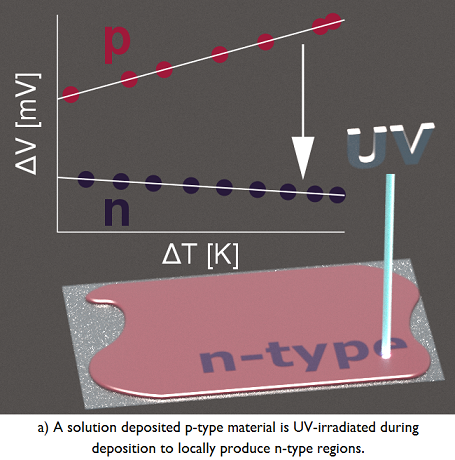
The fabrication processes of n- or p-type semiconducting devices usually require the deposition of both, n- and p-type materials, which have different processing requirements. In the proposed method, only one solution of a p-type material has to be deposited. Subsequently, it can locally be irradiated with light to convert the material to n-type according to the needs (Fig. a).
Because the deposition itself comprises only a single step, this automatically ensures good electrical as well as physical contact between n- and p- regions, thereby minimizing contact resistance and avoiding dewetting and delamination issues. All of this allows to reduce the minimum process complexity, by not only forgoing the deposition step for the complementary semiconductor layer, but also potentially avoiding the need for further deposition steps of metallic interconnect layers in some devices like thermoelectric generators. Another advantage of patterning using light instead of additive techniques like inkjet printing, is the strongly increased resolution that photolithography offers.
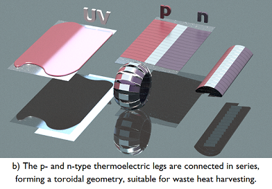
Application to thermoelectricity has been demonstrated, using a large-scale, roll-to-roll coating compatible in-plane geometry that showcases the convenience of the developed method, while also using the inherent advantages of flexible substrates to their fullest (Fig. b).
Advantages and Innovations
•	Very simple fabrication processes, to keep costs low.

•	Large areas can be coated and then patterned using optical techniques instead of relying on more complicated and less accurate multi-step printing processes.

•	Higher thickness homogeneity compared to additive manufacturing.

•	Applicability goes well beyond the area of thermoelectric power generation, and will prove useful in other fields, such as large area Peltier coolers, intelligent insulation materials, smart textiles, printed electronics in general.

•	The materials used are stable in air over months.
Stage Of Development
Available for demonstration
Requested partner
We are looking for industrial partners from the Printed electronics sector, companies interested in the use and explotation of this fabrication method, under patent license.
Cooperation offer is closed for requests